
Main
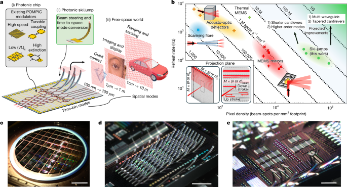
The transmission of information in our universe—from the astronomic to the atomic—is mainly photonic. Although most of our digital data travel through photonic waveguides, a far larger data stream is transmitted photonically in the free-space world. An efficient chip-to-world photonic interface—that is, the ability to convert between the time-bin modes of an integrated electro-optic processor and the spatial modes of free space—creates opportunities in communications and ranging3,5,6,7, additive manufacturing8, near-eye displays9,10, biomedical imaging11,12, machine learning13 and atom control for quantum information14. However, our current digital infrastructure struggles with the immense data streams from the real world, in which every resolvable pixel is a channel that must be processed15. A similar challenge exists in quantum computing, which requires photonic control and readout of millions of physical qubits to achieve fault tolerance16. Concurrently, photonic integrated circuits (PICs) have proliferated17 and demonstrated sophisticated functionalities, including light conditioning for atomic arrays14 and free-space displays, in-physics algorithms13 and deep co-learning at the edge18. As digital electronics become more intelligent, the chip-to-world optical interface becomes a crucial link in the digital intelligence value chain.
Despite this, the lack of a mode-efficient interface between the guided-wave modes of PICs and the continuous modes of free space has prevented their seamless and scalable use. Integrated waveguide systems possess a large number of time-bin modes due to rapid electro-optic and all-optical interactions19, but have a limited number of waveguide modes, with broadband, diffraction-limited input or output available only at the chip edge20. By contrast, free space offers a nearly unbounded number of spatial modes21 with slower temporal variations for many applications3,4,9,22. Although the total mode counts are similar, existing solutions fail to bridge this mismatch due to poor mode quality1, limited fields of view (FOV), slow scan rates or a lack of direct, scalable PIC integration3,9,11,23,24. The ideal solution requires the ability to project and scan a diffraction-limited, single-mode beam to: (1) a large number of resolvable beam-spots N in the far field, (2) with a high refresh rate, (3) from a limited footprint and (4) directly on the surface of a programmable photonic chip. Current beam-scanning architectures face a fundamental trade-off: tiled aperture devices3 and optical phased arrays5 offer programmability but suffer from diffraction-degraded beam quality, whereas continuous aperture scanners11,25 are constrained by inertial limits and integration challenges. Consequently, existing solutions lack the ability to project scannable, broadband, non-diffractive emission directly from the chip surface2 (refer to Supplementary Section 8 for detailed architectural comparisons).
Although it is challenging to distil a single figure of merit (FOM) that captures all facets of a laser scanning system’s size, weight, power and cost, the per-footprint-area resolvable spot count is a foundational metric that not only determines the number of devices per wafer, but also has downstream effects on all of these key performance metrics. For our analysis, we quantify performance by taking the product of this footprint-adjusted spot count and the refresh rate, yielding a net FOM in units of spots s–1 mm–2. This simplified metric provides a baseline for comparison among different technologies26. Conventional pupil-plane scanners require large apertures for high resolution, which leads to slow, high-power actuation that limits FOMs to between approximately 500,000 and 1 million spots s–1 mm–2. By contrast, focal-plane scanners decouple optical and mechanical dimensions, but the use of bulk components has limited their FOM to fewer than 50,000 spots s–1 mm–2. Thus, the focal-plane scanning approach has been hindered by the lack of a scalable, actuatable single-mode waveguide that can be integrated directly on a PIC.
Here we introduce a new class of integrated photonic devices—the photonic ski-jump—that overcomes these challenges and enables a scalable chip-to-world photonic interface (Fig. 1a). This device, fabricated on a 200-mm wafer in a volume complementary-metal–oxide–semiconductor (CMOS) foundry, is composed of a nanoscale optical waveguide embedded monolithically on a piezoelectrically actuated microcantilever with submicrogram mass, thickness of about 2 µm and a large out-of-plane curvature. The small mass and physical dimensions overcome the inertial limits of scanning fibres and break the FOM trade-offs of pupil plane scanners. The large upward curvature is achieved by engineering the directionality of the intrinsic material stress differential between the thin film layers of the cantilever bimorph27 (Supplementary Section 1)—an approach inspired by mechanical metamaterials28 and which has been demonstrated on other quantum photonic platforms29. This provides vertical, scannable, broadband optical emission from anywhere on a 200-mm wafer with mechanical resonances from about 1 kHz to over 100 kHz, which significantly enhance the scan speed and FOV. The submicrometre integrated waveguides simultaneously minimize the mass and emitted spot-size, resulting in a greater-than-1,000-fold FOM improvement over existing fibre scanners11,25 and a greater-than-50-fold FOM improvement over mature micro-electro-mechanical systems (MEMS) mirrors3,4 and acousto-optic deflectors23,26,30 (Fig. 1b).

a, (i) Existing piezoelectric POMPIC components14,31,32,33,34 enable fast photonic control and information processing over many time-bin modes on a scalable photonics platform. (VL)π is the voltage–length product to achieve a π phase shift. (ii) Photonic ski-jumps enable beam-scanning and time-to-space mode conversion directly from the surface of a photonic chip. (iii) Targets in the free-space world have many spatial modes with slow temporal evolution. b, Comparison of the photonic ski-jump with leading laser beam scanners as a function of footprint-adjusted pixel density and refresh rate. Footprint refers to the active beam-scanner device area. Data points (green circles) are obtained from a single ski-jump measured in vacuum at 1, 2, 5 and 10 volts peak-to-peak (Vpp; left to right). Lower-left inset: projection plane FOV is given by the scan angle θ for pupil plane scanners or scan distance d for focal plane scanners scaled by magnification M. Acousto-optic deflector data points are from refs. 23,26,30. The MEMS mirror data points are the highest-performing devices from table 4 in ref. 3. The scanning fibre is from ref. 25 and the thermal MEMS is from ref. 2. c, A diced, unreleased POMPIC wafer. Scale bar, ~5 cm. d, A 64 ski-jump array on a POMPIC. Scale bar, 1 mm. e, Photonic ski-jumps integrated with other POMPIC components. Scale bar, 1 mm.
Photonic ski-jumps are members of a unified family of active components on a CMOS-compatible piezo-opto-mechanical photonic integrated circuit (POMPIC) platform. Past works on this platform are shown in Fig. 1a and include tunable directional couplers31, phase shifters32,33, programmable Mach–Zehnder interferometers32,34 and tunable ring resonators14,32. This extensive process development kit allows for complex photonic processing upstream of the ski-jump on the same monolithic photonic platform (Fig. 1c–e). Ski-jumps are also cryogenically compatible for direct integration with solid-state qubit systems such as colour centres in diamond, which have been heterogeneously integrated onto the POMPIC platform for microwave and strain control35. This opens up new routes for the addressing and readout of spin qubits. Future integration with electro-optic thin films36 could enable 100 GHz modulation for the projection of subnanosecond optical pulses. The capabilities of the POMPIC platform combined with the chip-to-world projection capability of the ski-jump enables scalable photonic and quantum control on- and off-chip.
Device overview
Scalability and mode quality are crucial to the practical implementation of a chip-to-world photonic interface. Photonic ski-jumps are fabricated using a 200-mm CMOS foundry process that combines silicon nitride (Si3N4) photonics with mature aluminium nitride (AlN) piezo-actuators (Fig. 2a). Applying voltage across the aluminium electrodes induces piezoelectric stress in the AlN layer causing the ski-jump to deflect. The waveguides—composed of a Si3N4 core and SiO2 cladding—are patterned at the top of the layer stack33 and can be tailored for broadband, single-mode (or multimode) propagation across the visible-to-telecom spectrum37. We further tailor the passive curl of the ski-jump by engineering an oxide cross-rib pattern perpendicular to the waveguides (Fig. 2a–f and Supplementary Section 1). The devices studied here have Si3N4 waveguides (400 nm wide and 300 nm thick) that are designed for single-mode propagation at around 737 nm, the zero-phonon line of silicon vacancy colour centre emitters in diamond. The spot-size and numerical aperture of the ski-jump’s optical output can be optimized for the intended application by tapering the waveguide width at the cantilever tip. For the devices discussed in this work, the waveguide width tapers down to 200 nm at the tip, resulting in a beam-spot size (that is, mode field diameter) of ({d}_{mathrm{spot},x}) = 0.66 µm and ({d}_{mathrm{spot},y}) = 0.50 µm, and divergence half-angles of θx = 41° and θy = 53° for the fundamental transverse electric mode (Supplementary Section 9).

a, Conceptual overview. Magnified segment shows the cross-section composed of the lower layers (SiO2–Al–AlN–Al) and upper optical layers (Si3N4-in-SiO2). Each set of layers is about 1-μm thick, resulting in an approximately 2-μm-thick (h) cantilever. A small radius of curvature (R) is obtained by using cross-rib patterning of the top SiO2, which expands laterally (blue arrows) causing downward lateral curvature and lateral compression (red arrows) along with longitudinal expansion (blue arrows) of the lower layers, resulting in upward longitudinal curvature. Upper-right inset: scanning electron microscope image demonstrating downward lateral curvature of the cantilever. Lower-left inset: finite-element method simulation of the transverse electric single-mode profile along the waveguide operating at 737 nm. Lower-right inset: conceptual diagram of differential strain (ε) between the top and bottom layers. b,c, Scanning electron microscope images of cantilevers without (b) and with (c) cross-ribs to suppress lateral upward curvature and enhance longitudinal curvature. Scale bars, 200 μm. d, Variation of curvature with cross-rib period (P), cantilever width (W, in micrometres) and waveguide count (N). Scale bars, 500 μm. e, Scanning electron microscope images of cross-rib patterning with varying periods. f, Longitudinal curvature of cantilevers with 0.75-μm-wide cross-ribs with periods ranging from 4 to 64 μm. g, Direct current actuation measured using white-light profilometry for −50 V to 50 V. Inset: radius of curvature for each dataset as a function of the applied direct current voltage. The measured longitudinal displacement range is about 29.4 μm.
Direct current and resonant one-dimensional scanning
Scanning a waveguide in space naturally implements conversion between waveguided time-bin modes and spatial modes in the continuum. Direct current actuation (Fig. 2g) can be a useful means for tuning the ski-jump’s curvature and tip displacement to optimize coupling to: free-space optics, optical fibres, directly to free-space targets or to other PICs. Ski-jump power consumption is exceptionally low, with an approximately 10 nW (20 V) direct current hold power (Supplementary Section 5).
Each device also exhibits mechanical resonances that substantially enhance longitudinal and lateral displacement. The frequency and shape of these modes are determined by material stress, stiffness and device geometry38, with finite-element method results (Fig. 3a) that agree with the characteristic modes of a passively curled, singly clamped cantilever38. Given that the bending dimension is along the film thickness, most resonances within the simulated frequency range are longitudinal (Y). For lateral (X) modes, the bending dimension is along the cantilever width, which results in higher effective stiffness and resonance frequencies. Like other focal plane scanners, these devices scan both angle and displacement depending on the trajectory of the excited modes. We characterize the alternating current response of a device at various pressures and in cryogenic conditions (6.9 K) while driven with sinusoidal voltages with amplitudes up to 80 Vpp in ambient conditions and up to 10 Vpp in vacuum (Fig. 3) (refer to Supplementary Section 3 for details on the experimental set-up).

a, Finite-element method simulations for seven of the resonant modes of a curled cantilever (L = 950 μm, W = 70 μm). Below: stroboscopic images of a resonantly driven ski-jump. b–f, Intensified charge-coupled device (ICCD) images of the waveguide output on-resonance (Y1 ≈ 1.3 (b), Y2 ≈ 6.5 (c), X1 ≈ 4.9 (d), Y1 = 1.25 (e) and Y2 = 6.5 (f) kHz) with various sinusoidal drive voltages (streak labels in Vpp) for a device with dimensions L = 950 μm and W = 70 μm. The first two longitudinal modes and the first lateral mode are in high-vacuum (b–d) or ambient (e,f) conditions. In b–d, approximate frequencies are given as resonance frequency shifts with voltage due to thermal redshifting. The exposure time is greater than the drive signal period so that the full range of motion is observed. Time-resolved motion was also recorded using high-speed gating of the ICCD (Supplementary Video 4). g, Optically broadband operation of a ski-jump on-resonance (Y2 = 6.75 kHz, 40 Vpp), under ambient conditions. h,i, Small-signal frequency response of X and Y beam displacement. Measurements were taken with the device at room temperature under atmospheric pressure, rough vacuum or high vacuum (h), and cryogenic conditions under high vacuum (i). Data are normalized to the Y displacement at low frequencies. j, Ring-down measurement for the fundamental longitudinal mode under high vacuum at room temperature.
On resonance, ski-jumps exhibit varying degrees of out-of-plane (Z) motion depending on the mechanical mode profile, as shown in stroboscopic imaging of the resonance mode profiles (Supplementary Videos 1–3). For example, the fundamental Y mode (Y1) scans the cantilever tip along a nearly circular arc. By contrast, higher-order resonances such as the second-order Y mode (Y2) exhibit much lower Z and angular motion due to the additional motional nodes. This separates the cantilever into distinct segments with opposing changes in curvature such that the composite motion results in a nearly flat tip trajectory while remaining nearly vertically oriented. Similarly, the fundamental X mode (X1) exhibits a nearly flat tip trajectory due to the small passive curvature along the X direction. We also find good agreement between the analytically derived expression for FOM1D and the data for the Y2 mode (Supplementary Section 8). Furthermore, the ski-jump’s broadband transmission (450 nm to 750 nm) is demonstrated on-resonance using a supercontinuum source (Fig. 3g).
Decreasing the pressure substantially enhances the resonant response (by up to 30 dB). In high vacuum, the Y1 mode has a quality factor (Q) of approximately 10,020, demonstrating displacements similar to ambient conditions (Q ≈ 5) with approximately one-hundredth of the voltage. In vacuum, we observe a red-shifting nonlinearity due to electromechanical heating that passively stabilizes the drive frequency-resonance detuning, similar to other micro-oscillator systems19,39, and also substantially expands the resonance bandwidth. We measure the phase response and demonstrate a proportional-integral-derivative (PID)-based control loop to automatically find and track resonances and show that the frequency and resonantly enhanced scan ranges are stable after reaching a steady state (Supplementary Section 16).
Resonant two-dimensional beam scanning and image projection
At the core of a chip-to-world photonic interface is the ability to project a large two-dimensional array of beam-spots in the far-field. To this end, we use a ski-jump with bilateral piezoelectric actuators (Fig. 4a). Each electrode can be driven at multiple frequencies with different voltages and relative phases to enable the excitation of both X and Y resonances simultaneously, resulting in Lissajous curves with varying refresh rates and beam-spot densities depending on the particular frequency ratio22. We characterize the X and Y frequency response of the device from 100 Hz to 50 kHz with separate, same-frequency signals sent to the two actuators while measuring the projected beam displacement with a position-sensitive detector (Fig. 4d). Mechanically, driving out-of-phase signals cancels out the Y response while enhancing the X response. This enables cancellation of X–Y cross-coupling and efficient driving of the two orthogonal axes for 2D beam-scanning. Optically, the combination of the second-order Y mode and fundamental X mode exhibits a sufficiently flat 2D scan area to serve as the basis for projecting a large 2D array of near diffraction-limited beam-spots.

a, Top-down SEM image of a split-electrode cantilever’s base. False colour added to show left (purple) and right (cyan) electrodes. b, ICCD images of the split-electrode ski-jump’s optical output tracing Lissajous patterns while the cantilever (L = 950 μm, W = 70 μm) is driven at different X:Y frequency ratios (4.83 kHz:6.44 kHz = 3:4 with a 1.61 kHz refresh rate, top row; and 37.2 kHz:6.2 kHz = 6:1 with a 6.2 kHz refresh rate, bottom row) and phase offsets of φ = 0 (left), φ = π/2 (middle) and φ = π (right) between the X and Y drive signals. c, Tuning of the 2D scan area by varying amplitudes AL and AR with the left and right actuators driving near 4.83 kHz and 6.5 kHz, respectively, in high-vacuum conditions. Resonance frequencies shift slightly depending on the voltage. d, Frequency response of the X and Y beam displacement while driving both actuators with in-phase (top) and out-of-phase (bottom) sinusoidal signals of 1 Vpp in ambient conditions. e, Diagram of 2D image projection with a split-electrode device, controlled by an arbitrary waveform generator (AWG) or a field-programmable gate array (FPGA). Purple and cyan insets: a ski-jump projecting the letters ‘QMP’ (Quantum Moonshot Project). f, Image projection using a long split-electrode device (L = 1,450 µm, W = 70 µm) tracing full-fill Lissajous patterns in vacuum conditions with fx = 1.561 kHz, fy = 2.639 kHz and a refresh rate of 7 Hz. g, Image projection using a shorter split-electrode device (L = 950 µm, W = 70 µm) in vacuum conditions with fx = 4.716 kHz, fy = 6.408 kHz and a refresh rate of 36 Hz. Institution logos used with permission from MITRE, MIT, Sandia National Laboratories and the University of Arizona, respectively. Video projections (36 Hz) are provided as Supplementary Videos 6 and 7. Colour projection examples were not modified post-capture. The camera’s exposure time matches the ski-jump’s refresh rate.
The choice of frequencies for the X and Y signals dictates both refresh rate and fill factor for the scan pattern. Applications such as LiDAR and image projection require high-fill, low-rate patterns, whereas low-fill, high-rate patterns are more suitable for optical control of atomic qubits. We generate high-refresh-rate Lissajous patterns by applying X and Y signals with low-frequency ratios and adjusting their relative phase (Fig. 4b and Supplementary Video 5). Offsetting one of the frequencies sweeps the beam across the entire 2D area (Fig. 4c) with a low refresh rate that is equal to the greatest common divisor of the X and Y frequencies. By pulsing the optical signal with off-chip current-controlled laser diodes, we demonstrate the projection of full-colour 2D images and video using these high-fill scans (Fig. 4e–g, and Supplementary Videos 6 and 7) without the need for active stabilization, indicating that the trajectories are stable over time. We also demonstrate excellent long-term stability of both high-rate and high-fill scan patterns while driving for over 15 h. The devices similarly exhibit long-term stability for direct current and one-dimensional resonant operation. Specifically, we observe no hysteresis for high-voltage direct current actuation and demonstrate one-dimensionally resonant scan stability over one billion cycles and over dozens of hours (Supplementary Section 12). Although we currently modulate the lasers off-chip, phase and amplitude modulation using our existing POMPIC components is readily achievable to enable all-on-chip projection systems.
Ski-jump excitation of silicon vacancy colour centres
To achieve a truly universal chip-to-world photonic interface, the projected light must control matter at the quantum mechanical level; that is, it must be spatially and spectrally coherent. This ability is central for the photonic control of atomic qubits and for applications across spectroscopy, fluorescence-based microscopy, and coherent ranging and sensing. To demonstrate this capability, we use a single ski-jump to control many solid-state atom-like qubits. Past work used a controllable Mach–Zehnder interferometer mesh to route input laser light into four discrete channels for spatially and temporally resolved control of quantum memories40. In contrast, the ski-jump has a continuous 2D range of outputs to control quantum memories as nodes on a grid. As such, the number of channels available scales based on the ski-jump’s range of motion and optical mode size.
We demonstrate this capability using a wirebonded, fibre-packaged ski-jump scanning along one dimension in ambient conditions. A diamond quantum microchiplet consisting of eight waveguides with implanted negatively charged silicon vacancies is placed in a Montana 4 K cryostat overhanging a bare silicon substrate (Fig. 5a). Laser light resonant with the silicon vacancy zero phonon line at ~737 nm is routed from the end of the ski-jump in free-space to the tips of the individual diamond waveguides.

a, Experimental set-up for projecting the ski-jump’s optical output onto a diamond quantum microchiplet with implanted silicon vacancies and readout onto a photodetector (APD or ICCD). b, Measurement of the second-order autocorrelation function g(2)(τ) for a single emitter in one of the diamond waveguides. At time τ = 0, we observe a visibility of g(2)(0) = 0.09(9), indicating that a single emitter is being addressed. c, Time-dependent PSB fluorescence of the single emitter excited via the cantilevered waveguide oscillating at 6.34 kHz. The emitter is positioned at the apex of the device’s range of motion. The extinction ratio is 27.5 dB with a repetition time of 157 μs. d, Ensemble fluorescence measurements collected with an ICCD. The driven cantilever addresses emitters in six distinct waveguides. The third waveguide, imaged at t = 39 μs, has a damaged taper. As a result, the resonant excitation was mostly scattered.
We align the emission of the static ski-jump with one of the diamond waveguide channels and tune the excitation laser to excite the C transition of a frequency-resolved single silicon vacancy colour centre. We verify that a single emitter is being addressed by performing a second-order autocorrelation measurement with g(2)(0) = 0.09(9), which is well below the 0.5 threshold for single photon emission (Fig. 5b). To periodically initialize this emitter, the ski-jump is driven to oscillate at 6.34 kHz while the silicon vacancy phonon sideband (PSB) fluorescence is routed to an avalanche photodiode coupled (APD) to a time-tagger (Fig. 5c). We observe consistent sideband emission with an extinction ratio of 27.5 dB, currently limited by scattered light. The standard deviation of the integrated pulse area is 0.003. We also demonstrate the control of multiple emitters in different waveguide channels by tuning the laser to a frequency that excites ensemble silicon vacancy and scanning the ski-jump’s optical output across the channels. We collect the PSB signal from each waveguide onto a high-speed ICCD, showing their real-time counts as the beam-spot scans over them (Fig. 5d).
This demonstration is a key link toward universal fault-tolerant quantum computation, which requires scalable, high-fidelity addressing of millions of qubits—a feat that is impractical with traditional bulk optics and acousto/electro-optic modulators. On-chip modulators alone are also insufficient without a scalable broadcast method. Our work provides this solution: a high-yield, PIC-based platform that integrates modulators and scanners to control thousands of optical channels per ski-jump. The co-integration of modulators and scanners on a single chip also provides a high level of phase stability between all channels unobtainable with bulk and fibre-based components40. Furthermore, cryogenic operation enables a modular architecture wherein the photonics control system can occupy a warmer stage of the cryostat while still being co-packaged with the qubits into a unified quantum processor unit. Practical architectures will probably require arrays of smaller ski-jumps that can cyclically and simultaneously excite a subset of the qubit array with submicrosecond refresh rates and dynamical shifting of the scan trajectory to interlink the qubit sub-arrays.
Discussion
Bypassing the inertial trade-off between actuator mass and optical aperture enables beam-spot densities and scan speeds beyond those of conventional scanners. The one-dimensional scaling laws (Supplementary Section 8)—FOM1D,Y ∝ QL (Wh2dspot,y)–1 and FOM1D,X ∝ QL (W2hdspot,x)–1—favour longer, thinner cantilevers with a tapered or segmented width profile to minimize air damping. This approach increases both scan speed and range but reduces the refresh rate (Fig. 1b) because the 2D spot density scales faster (bilinear) than scan speed (Euclidian) as a function of the 1D scan ranges. A similar tradeoff exists optically: the untapered waveguide cross-section reduces the beam-spot diameter by ~40% and yields a 2.8× increase in spot density (spots mm–2) but only a 1.7× increase in scan speed (spots s–1). However, the flexibility of Lissajous scanning allows the ski-jump to dynamically trade off fill-factor for refresh-rate by choosing a frequency pair with a larger greatest common divisor and therefore higher refresh-rate, though this trade-off degrades for increasingly sparse patterns. Alternatively, integrating multiple waveguides onto each cantilever will also boost the fill-factor-refresh-rate product proportionally, but at the cost of more individual optical channels to modulate and route. Practically, the scan range, speed, pattern, waveguide placement and spot-size can be co-optimized to match the target illumination pattern and clock-rate.
Interfacing with centimetre-scale ski-jump arrays also pushes the limits of standard optics. However, high-volume, precision-moulded free-form optics—like those in modern phone cameras—now provide near-diffraction-limited performance at consumer cost. Leveraging optical reciprocity, these micro-optics can collimate approximately 1-µm spot-size ski-jump arrays within a sub-one-centimetre-cubed module. We validate this with an iPhone 15 Pro lens, producing an image with a 1.69 µm Airy radius, matching the Rayleigh resolving limit (modulation transfer function = 0.10) of 1.67 µm for the f/1.78 lens (Supplementary Section 13). Analysis of the lens specifications41 predicts approximately 30 M resolvable spots over a 12.2 mm diameter, accommodating over 1,000 ski-jumps. For monochromatic applications like eye-safe LiDAR, a single-element fish-eye metalens (demonstrated at 940 nm (ref. 42) and 1,550 nm (ref. 43)) provides a compact, wafer-level solution for near-diffraction-limited imaging over a 170° FOV. A single metalens with <0.1° angular resolution covers >175 ski-jumps, simplifying packaging to one monolithic component. At the opposite scale, micro-lens arrays offer lens-per-emitter control44. Tiled over the wafer, each micro-lens array cell couples a ski-jump to a lenslet, enabling composite imaging that removes inter-ski-jump gaps or light-field architectures that add varifocal or volumetric capabilities. Supplementary Section 14 details the beam-spot capacity and volume of such packaged systems. To demonstrate realistic uniformity and yield of arrays, we fabricated a 64 ski-jump array and measured a curvature distribution with a standard deviation of <2% (Supplementary Section 18). This compact tiling, combined with a 10× increase in the ski-jump FOM, would enable giga-spot light engines at 1kHz refresh rates in a sub-5-cm diameter chip area.
Scaling these devices into integrated systems requires addressing several additional constraints. The ski-jump’s curved scan trajectory can cause defocusing in optics designed for flat sensors, a challenge addressable with optical45 and mechanical38,46 compensation (Supplementary Section 13). Other considerations include die-level vacuum packaging, which provides the necessary low-pressure environment without bulky chambers47,48; however, future actuator design improvements will narrow the performance gap for ambient operation. Also, while resonant scanning lacks true random access, a large ski-jump array enables coarse pointing by simply switching emission among different devices, each independently tunable within its direct current range. Higher optical powers may introduce waveguide nonlinearities or thermal loading, which can be mitigated with established control and heat-management methods49. Despite these constraints, the design flexibility of this platform underscores the ski-jump’s transformative potential.
Conclusion
Ski-jumps mark a significant advancement toward bridging the gap between integrated photonic circuits and the free-space world. By directly integrating low-mass, high-NA waveguides onto a chip-based piezo-cantilever, we overcome key inertial and diffraction trade-offs that have long hindered conventional beam-scanning technologies. Although our current implementations rely on resonant scanning in vacuum for optimal performance, there are clear, practical avenues for future refinement. More importantly, establishing a robust chip-to-world photonic interface opens up exciting opportunities for machine vision and intelligence across applications such as autonomous vehicles, robotics, augmented reality, biomedical imaging and laser-based lithography. We anticipate this technology will form the basis of a light engine that enables machines to sense, communicate and interact more effectively with their environment and with one another—ultimately enhancing human productivity and connectivity in our increasingly information-driven world.
Methods
Device fabrication and input–output
The fabrication process follows the approach laid out in ref. 32. A cross-section schematic is provided in Supplementary Fig. 1. Cantilevers are fabricated on a CMOS platform with a silicon substrate. After an initial SiO2 deposition, an amorphous silicon layer is deposited below the cantilever. The next layers are SiO2, Al, AlN, Al, SiO2, Si3N4 and, finally, SiO2. A defined etch around the cantilever exposes the underlying amorphous silicon. Release holes are patterned every 30 μm along the length and width of the cantilever to ensure a complete release. After wafer fabrication is complete, the PICs are placed in a XeF2 gas-etching chamber that etches away the amorphous silicon, releasing the cantilever except for a clamp at one end. The inherent stresses in the overlying thin films, along with tailored cross-rib patterning in the top SiO2, causes the cantilever to curl out of the PIC plane. The standard Si3N4 waveguides used on these devices were 400-nm wide and 300-nm thick. There is an approximately 400-nm SiO2 wide cladding buffer on the left and right sides of the waveguide(s), along with a top SiO2 clad thickness of around 400 nm and a bottom SiO2 clad thickness of around 850 nm.
Pads for electrical contact use routing metal and tungsten vias to independently route signals to the top and bottom electrodes of the single electrode cantilevers. The split-electrode devices share a ground plane but use independent signal pads to control the left and right actuators. Electrical signals are sent to these pads using GSG(SG) probes or via wirebonds to a custom PCB. Laser light is routed to the ski-jumps either using an edge-coupled lensed fibre or a fully packaged fibre-to-grating coupler system.
Data availability
The data that support the plots and findings within this paper are available from the corresponding authors on request.
References
-
Hsu, C.-P. et al. A review and perspective on optical phased array for automotive LiDAR. IEEE J. Sel. Top. Quantum Electron. 27, 1–16 (2021).
-
Sharif Azadeh, S. et al. Microcantilever-integrated photonic circuits for broadband laser beam scanning. Nat. Commun. 14, 2641 (2023).
-
Wang, D., Watkins, C. & Xie, H. MEMS mirrors for LiDAR: a review. Micromachines 11, 456 (2020).
-
Hofmann, U., Janes, J. & Quenzer, H.-J. High-Q MEMS resonators for laser beam scanning displays. Micromachines 3, 509–528 (2012).
-
Poulton, C. V. et al. Coherent LiDAR with an 8,192-element optical phased array and driving laser. IEEE J. Select. Topics Quantum Electron. 28, 6100508 (2022).
-
Zhang, X., Kwon, K., Henriksson, J., Luo, J. & Wu, M. C. A large-scale microelectromechanical-systems-based silicon photonics LiDAR. Nature 603, 253–258 (2022).
-
Li, B., Lin, Q. & Li, M. Frequency-angular resolving LiDAR using chip-scale acousto-optic beam steering. Nature 620, 316–322 (2023).
-
Corsetti, S., Notaros, M., Sneh, T., Page, Z. A. & Notaros, J. Silicon-photonics-enabled chip-based 3D printer. Light Sci. Appl. 13, 132 (2024).
-
Hsiang, E.-L. et al. AR/VR light engines: perspectives and challenges. Adv. Opt. Photon. 14, 783 (2022).
-
Li, Z. et al. Meta-optics achieves RGB-achromatic focusing for virtual reality. Sci. Adv. 7, eabe4458 (2021).
-
Lee, C. M., Engelbrecht, C. J., Soper, T. D., Helmchen, F. & Seibel, E. J. Scanning fiber endoscopy with highly flexible, 1 mm catheterscopes for wide-field, full-color imaging. J. Biophoton. 3, 385–407 (2010).
-
Sacher, W. D. et al. Implantable photonic neural probes for light-sheet fluorescence brain imaging. Neurophotonics 8, 025003 (2021).
-
Farmakidis, N., Dong, B. & Bhaskaran, H. Integrated photonic neuromorphic computing: opportunities and challenges. Nat. Rev. Electr. Eng. 1, 358–373 (2024).
-
Menssen, A. J. et al. Scalable photonic integrated circuits for high-fidelity light control. Optica 10, 1366–1372 (2023).
-
Kaufmann, E. et al. Champion-level drone racing using deep reinforcement learning. Nature 620, 982–987 (2023).
-
Fowler, A. G., Mariantoni, M., Martinis, J. M. & Cleland, A. N. Surface codes: towards practical large-scale quantum computation. Phys. Rev. A 86, 032324 (2012).
-
Bogaerts, W. & Rahim, A. Programmable photonics: an opportunity for an accessible large-volume PIC ecosystem. IEEE J. Sel. Top. Quantum Electron. 26, 1–17 (2020).
-
Sludds, A. et al. Delocalized photonic deep learning on the internet’s edge. Science 378, 270–276 (2022).
-
Joshi, C. et al. Thermally controlled comb generation and soliton modelocking in microresonators. Opt. Lett. 41, 2565 (2016).
-
Xiang, C., Jin, W. & Bowers, J. E. Silicon nitride passive and active photonic integrated circuits: trends and prospects. Photon. Res. 10, A82 (2022).
-
Panuski, C. L. et al. A full degree-of-freedom photonic crystal spatial light modulator. Nat. Photon. 16, 834–842 (2022).
-
Wang, J., Zhang, G. & You, Z. Improved sampling scheme for LiDAR in Lissajous scanning mode. Microsyst. Nanoeng. 8, 64 (2022).
-
Antonov, S. N. & Kotelnikov, V. A. A review of physical principles and applications of acousto-optic deflectors on the basis paratellurite. Phys. Astron. Intl J. 3, 62–65 (2019).
-
Zhang, B., Peng, P., Paul, A. & Thompson, J. D. A. Scaled local gate controller for optically addressed qubits. Optica https://doi.org/10.1364/OPTICA.512155 (2023).
-
Wang, W.-C. et al. Mirrorless MEMS imaging: a nonlinear vibrational approach utilizing aerosol-jetted PZT-actuated fiber MEMS scanner for microscale illumination. Microsyst. Nanoeng. 10, 13 (2024).
-
Römer, G. R. B. E. & Bechtold, P. Electro-optic and acousto-optic laser beam scanners. Phys. Procedia 56, 29–39 (2014).
-
Timoshenko, S. Analysis of bi-metal thermostats. J. Opt. Soc. Am. 11, 233 (1925).
-
Chen, S., Chen, J., Zhang, X., Li, Z.-Y. & Li, J. Kirigami/origami: unfolding the new regime of advanced 3D microfabrication/nanofabrication with ‘folding’. Light Sci. Appl. 9, 75 (2020).
-
Qvotrup, C. et al. Curved GaAs cantilever waveguides for the vertical coupling to photonic integrated circuits. Opt. Express 32, 3723–3734 (2024).
-
ODXY1441-T95S-3 (ISOMET, 2014); https://go.nature.com/4a2qt9c.
-
Wen, Y. H. et al. Tunable directional couplers in a scalable piezo-MEMS platform. In Frontiers in Optics + Laser Science 2023 (Optica, 2023); https://doi.org/10.1364/fio.2023.fth1e.4.
-
Stanfield, P. R., Leenheer, A. J., Michael, C. P., Sims, R. & Eichenfield, M. CMOS-compatible, piezo-optomechanically tunable photonics for visible wavelengths and cryogenic temperatures. Opt. Express 27, 28588–28605 (2019).
-
Dong, M. et al. High-speed programmable photonic circuits in a cryogenically compatible, visible–near-infrared 200 mm CMOS architecture. Nat. Photon. 16, 59–65 (2021).
-
Dong, M. et al. Piezo-optomechanical cantilever modulators for VLSI visible photonics. APL Photonics 7, 051304 (2022).
-
Clark, G. et al. Nanoelectromechanical control of spin–photon interfaces in a hybrid quantum system on chip. Nano Lett. 24, 1316–1323 (2024).
-
Valdez, F., Mere, V. & Mookherjea, S. 100 GHz bandwidth, 1 volt integrated electro-optic Mach–Zehnder modulator at near-IR wavelengths. Optica 10, 578 (2023).
-
Wen, Y. H. et al. Strain-concentration for fast, compact photonic modulation and non-volatile memory. Optica 11, 1511 (2024).
-
Rao, S. S. Vibration of Continuous Systems (John Wiley & Sons, 2007).
-
Carmon, T., Yang, L. & Vahala, K. Dynamical thermal behavior and thermal self-stability of microcavities. Opt. Express 12, 4742–4750 (2004).
-
Palm, K. J. et al. Modular chip-integrated photonic control of artificial atoms in diamond nanostructures. Optica https://doi.org/10.1364/OPTICA.486361 (2023).
-
Yao, Y., Shinohara, Y. & Liao, L.-Y. Imaging lens system. US Patent US11347030B2 (2022).
-
Shalaginov, M. Y. et al. Single-element diffraction-limited fisheye metalens. Nano Lett. 20, 7429–7437 (2020).
-
2Pi Optics (Private Communications, 2025).
-
Ingeneric Micro-lens Array Catalog (Ingeneric, 2023); https://go.nature.com/4c1QbgD.
-
Qin, Y., Chen, W.-Y., O’Toole, M. & Sankaranarayanan, A. C. Split-Lohmann multifocal displays. ACM Trans. Graph. 42, 57 (2023).
-
Xie, X. & Livermore, C. A high-force, out-of-plane actuator with a MEMS-enabled microscissor motion amplifier. J. Phys. Conf. Ser. 660, 012026 (2015).
-
Schott Hermetic Optical Enclosures Catalog (Schott, 2025); https://go.nature.com/3LIyckR.
-
Edinger, P. et al. Vacuum-sealed silicon photonic MEMS tunable ring resonator with an independent control over coupling and phase. Opt. Express 31, 6540–6551 (2023).
-
MEMS Mirrors (Hamamatsu, 2023); https://go.nature.com/3ZEPr9I.
Acknowledgements
Major funding for this work is provided by MITRE for the Quantum Moonshot Program. D.E. acknowledges partial support from Brookhaven National Laboratory, which is supported by the US Department of Energy, Office of Basic Energy Sciences, under contract no. DE-SC0012704 and the NSF RAISE TAQS program. M.E. performed this work, in part, with funding from the Center for Integrated Nanotechnologies, an Office of Science User Facility operated for the US Department of Energy Office of Science. Wes also thank L. Li and K. Chen for their fabrication of the silicon-vacancy-implanted diamond sample. We thank N. Otterstrom, S. Trajtenberg-Mills, T. Propson and X. Lu for valuable feedback on the manuscript. Y.M.G. and C.L. also acknowledge support from the US Department of Energy, Office of Science, National Quantum Information Science Research Centers, Quantum Systems Accelerator. Y.H.W. acknowledges J. Hu and Z. Li for insightful discussion and provision of micro-optic components. Sandia National Laboratories is a multimission laboratory managed and operated by National Technology & Engineering Solutions of Sandia, LLC, a wholly owned subsidiary of Honeywell International for the US Department of Energy’s National Nuclear Security Administration under contract DE-NA0003525. This paper describes objective technical results and analysis. Any subjective views or opinions that might be expressed in the paper do not necessarily represent the views of the US Department of Energy or the United States Government.
Ethics declarations
Competing interests
D.E. is a Scientific Advisor to and is a co-founder of Axiomatic_AI. The other authors declare no competing interests.
Peer review
Peer review information
Nature thanks Linjie Zhou and the other, anonymous, reviewer(s) for their contribution to the peer review of this work. Peer review reports are available.
Additional information
Publisher’s note Springer Nature remains neutral with regard to jurisdictional claims in published maps and institutional affiliations.
Supplementary information
Rights and permissions
Open Access This article is licensed under a Creative Commons Attribution-NonCommercial-NoDerivatives 4.0 International License, which permits any non-commercial use, sharing, distribution and reproduction in any medium or format, as long as you give appropriate credit to the original author(s) and the source, provide a link to the Creative Commons licence, and indicate if you modified the licensed material. You do not have permission under this licence to share adapted material derived from this article or parts of it. The images or other third party material in this article are included in the article’s Creative Commons licence, unless indicated otherwise in a credit line to the material. If material is not included in the article’s Creative Commons licence and your intended use is not permitted by statutory regulation or exceeds the permitted use, you will need to obtain permission directly from the copyright holder. To view a copy of this licence, visit http://creativecommons.org/licenses/by-nc-nd/4.0/.
About this article

Cite this article
Saha, M., Wen, Y.H., Greenspon, A.S. et al. Nanophotonic waveguide chip-to-world beam scanning. Nature 651, 356–363 (2026). https://doi.org/10.1038/s41586-025-10038-6
-
Received:
-
Accepted:
-
Published:
-
Version of record:
-
Issue date:
-
DOI: https://doi.org/10.1038/s41586-025-10038-6